
- What are lead frames?
- Why Lead Frames are Important in the Semiconductor Industry?
- What Materials Are Commonly Used to Make Lead Frames?
- What Are the Main Functions of Lead Frames in Electronic Components?
- What Technologies Are Used in the Cutting and Shaping of Lead Frames?
- What Are the Different Types of Lead Frames Available?
- Conclusion
- FAQ
Lead Frames 101: Everything You Need to Know
Lead frames are the backbone of semiconductor devices, acting as the bridge between microelectronic components and external circuits. These metallic structures not only support the silicon chip but also play a crucial role in heat dissipation and electrical conductivity. Essential for the functionality and reliability of semiconductor packages, lead frames ensure that your everyday electronic devices operate seamlessly and efficiently.
Keeping this momentum, let’s delve deeper into why these components are so vital. Stick around as we explore the materials, technologies, and types of lead frames that keep our electronic world running smoothly.
What are lead frames?
Lead frames are integral components of semiconductor packaging, designed to support and connect the silicon chip to larger electronic systems. These frames provide a sturdy scaffold for the chip while facilitating crucial connections through their leads to the external circuitry.
They play a pivotal role in electrical signal transmission, as well as in heat dissipation, which is critical for maintaining the overall integrity and performance of electronic devices.
By ensuring that the chip is physically stable and electrically connected, lead frames are a key element in the functionality of a wide range of electronic products.
Why Lead Frames are Important in the Semiconductor Industry?
Lead frames are essential in the semiconductor industry because they act as the foundation for microchips, which power virtually every electronic device we use. Without lead frames, there would be no reliable way to connect the tiny silicon chips to external circuits.
These frames ensure proper electrical contact, allowing signals to flow seamlessly between the chip and its environment.
Additionally, they help dissipate the heat generated by the chip, preventing overheating and potential damage. In short, lead frames are the unsung heroes that ensure our electronics are both functional and durable.
What Materials Are Commonly Used to Make Lead Frames?
The choice of materials for lead frames is crucial for ensuring durability, electrical conductivity, and heat resistance. Typically, lead frames are made from copper alloys because of their excellent conductivity, which allows for efficient signal transmission. Copper is often combined with other metals like nickel, silver, or gold to enhance its properties, such as corrosion resistance and overall strength.
In some cases, stainless steel or precious metals like gold are used for high-performance applications where reliability and longevity are critical. The material choice can vary depending on the specific requirements of the semiconductor package, but copper-based alloys dominate the market due to their balance of cost and performance.
What Are the Main Functions of Lead Frames in Electronic Components?
Lead frames serve several critical functions in electronic components, all of which contribute to the overall reliability and efficiency of semiconductor devices.
- Electrical Connection: The primary function of a lead frame is to establish electrical contact between the silicon chip and the external circuit. It ensures that the signals from the chip are transmitted smoothly to the larger electronic system.
- Mechanical Support: Lead frames physically support the semiconductor chip, holding it in place within the package. This structural role prevents damage to the delicate chip during handling and operation.
- Heat Dissipation: As electronic components generate heat, lead frames help dissipate that heat away from the chip, preventing overheating and ensuring the longevity of the device.
- Encapsulation: The lead frame helps in encapsulating the chip with materials like epoxy, providing protection from environmental factors such as moisture, dust, and mechanical stress.
Without these crucial functions, electronic components would struggle to perform efficiently or reliably.
What Technologies Are Used in the Cutting and Shaping of Lead Frames?
The production of lead frames involves precise cutting and shaping processes, ensuring they meet the exact specifications required for their applications. Two primary technologies are commonly used in this process: Stamping and Photochemical Etching.
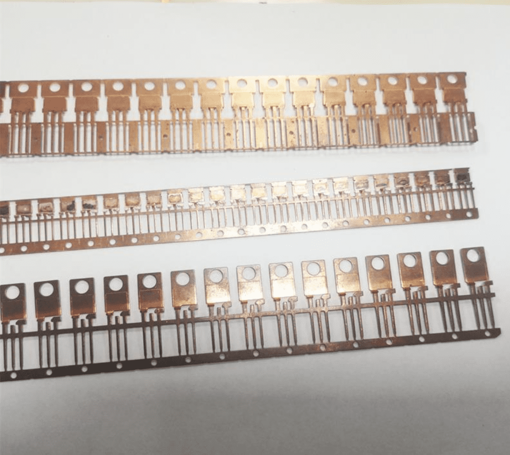
Lead Frame Stampings
Stamping is a widely used method in the manufacturing of lead frames, particularly when high volumes are needed. In this process, a metal sheet (typically copper alloy) is placed into a stamping die, where it is pressed and shaped into the desired form. The stamping process allows for highly accurate, high-speed production of lead frames, and it ensures consistent quality across large batches.
The benefits of stamping include:
- High Precision: Stamping allows for precise dimensions and shapes, essential for the delicate nature of semiconductor packaging.
- Cost-Effective: This method is ideal for mass production, as it reduces the need for extensive labor and tooling.
- Scalability: Stamping is efficient for large-scale manufacturing, making it suitable for industries that require thousands or even millions of lead frames.
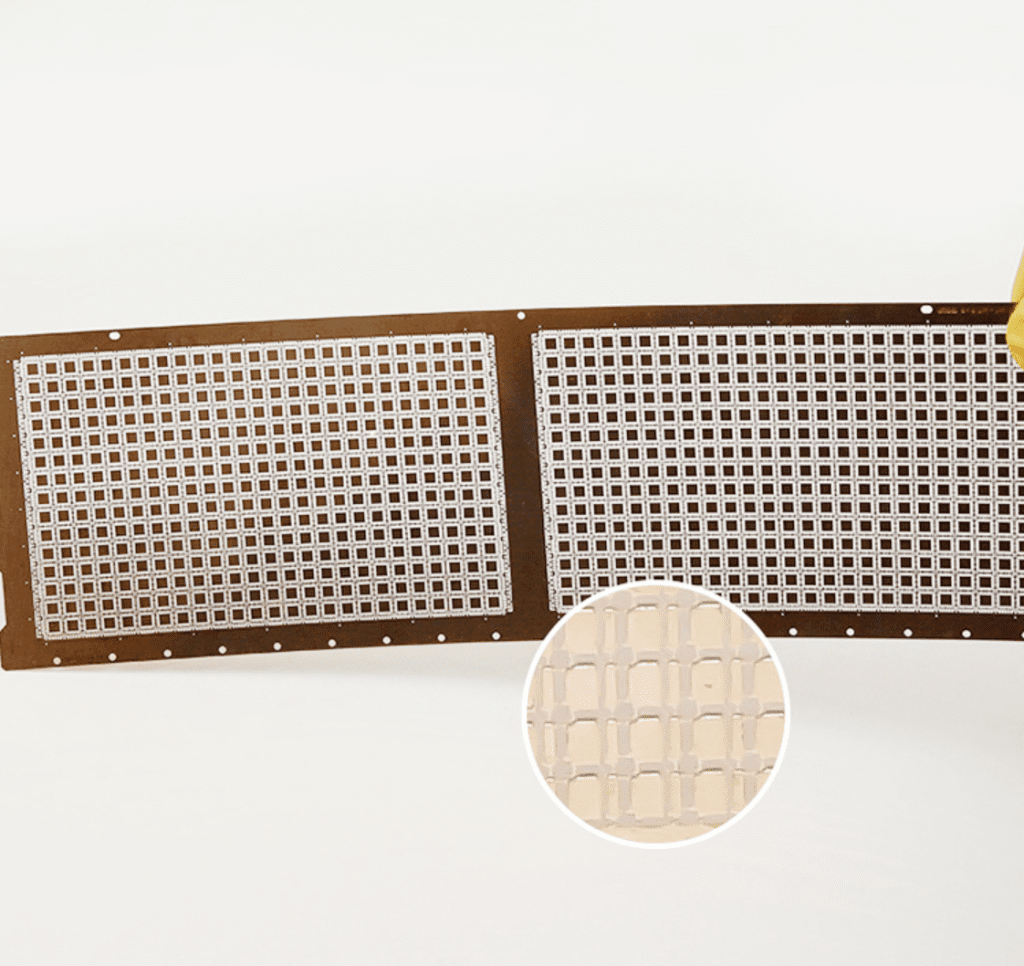
Lead Frame Photochemical Etching
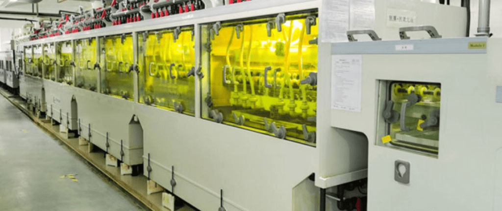
Photochemical etching (also called precision chemical machining, chemical blanking, or acid etching) is another advanced technology used for shaping lead frames, particularly when higher precision or intricate designs are required. This process involves using a photographic mask and a chemical etching solution to carve out specific patterns in the metal, typically copper or its alloys.
Here’s how it works:
- Masking: A thin layer of photoresist material is applied to the metal sheet. Then, a photomask, which contains the desired pattern, is aligned over the photoresist.
- Exposure: The assembly is exposed to ultraviolet (UV) light, which hardens the photoresist in the areas that are exposed to the light, while the unexposed areas remain soft.
- Etching: The metal sheet is then immersed in a chemical etching solution, which removes the unprotected areas of the metal, leaving behind the intricate design etched into the material.
- Finishing: After etching, the remaining photoresist is stripped away, revealing the finished lead frame.
The benefits of photochemical etching include:
- Precision: It allows for very fine details and tight tolerances, making it ideal for complex or miniaturized designs.
- Smooth Edges: The process results in smooth, burr-free edges, which are crucial for the delicate electrical contacts in semiconductor packages.
- Customizability: This method allows for the creation of highly customized lead frame designs with intricate geometries and specific features that may not be achievable with stamping alone.
While photochemical etching is typically more expensive and time-consuming than stamping, it’s perfect for high-performance applications where precision and design complexity are essential.
What Are the Different Types of Lead Frames Available?
1. Dual in-Line Package (DIP) Lead Frames
DIP lead frames are one of the most traditional types and are widely used for through-hole mounting of components on printed circuit boards (PCBs).
These lead frames feature two parallel rows of leads extending from the package, making them easy to insert into holes on the PCB.
They are commonly used in applications where a simple, reliable connection is needed, such as in low-to-medium power electronics.
2. Surface-Mount Package (SMD) Lead Frames
Surface-mount lead frames are designed for mounting components directly onto the surface of a PCB, rather than inserting them through holes.
These lead frames are ideal for compact, high-density electronic devices, as they reduce the overall size of the package and simplify the assembly process.
SMD lead frames are used in a wide range of consumer electronics, automotive, and telecommunications applications.
3. Chip-on-Board (COB) Lead Frames
COB lead frames are used in advanced semiconductor packaging, where the chip is directly mounted onto the board, eliminating the need for a traditional package.
These lead frames are typically used in high-performance applications such as LED lighting, sensors, and power devices.
They offer excellent heat dissipation and are ideal for compact designs where space and performance are critical.
4. QFN (Quad Flat No-lead) Lead Frames
QFN lead frames are used for quad flat no-lead packages, which feature leads underneath the package instead of the sides.
These lead frames are widely used in applications requiring a smaller form factor, such as mobile devices, networking equipment, and consumer electronics.
The design helps achieve better thermal performance and lower inductance, making QFN lead frames ideal for high-speed, high-frequency applications.
5. BGA (Ball Grid Array) Lead Frames
BGA lead frames are used for ball grid array packages, which have an array of solder balls underneath the package.
These lead frames are designed for high-density applications, providing excellent electrical performance and heat dissipation.
BGAs are commonly used in processors, memory chips, and high-performance computing systems. The ball grid design ensures reliable connections while maintaining a low-profile package.
6. SOT (Small Outline Transistor) Lead Frames
SOT lead frames are designed for small outline transistors, which are used in low-power applications like signal processing, switching, and amplification.
These lead frames are typically smaller than other types and are ideal for compact devices where space is at a premium.
SOT lead frames are widely used in consumer electronics, automotive, and telecommunications.
7. SOIC (Small Outline Integrated Circuit) Lead Frames
SOIC lead frames are designed for small outline integrated circuits, which are used in a variety of electronic systems, including automotive, medical devices, and industrial applications.
These lead frames offer a balance between size and performance, making them suitable for both low- and medium-power applications.
8. FLATPACK Lead Frames
Flatpack lead frames are used in packages that have leads extending from the sides of the package. This design is typically employed in larger, more robust packages that require strong electrical connections and mechanical support.
Flatpack lead frames are often found in industrial applications, power devices, and military electronics.
Conclusion
Understanding lead frames is crucial for anyone involved in the semiconductor industry, as they play an indispensable role in the performance and reliability of electronic components. If you’re looking for high-quality lead frames for your applications, feel free to contact us today. We’re here to provide expert solutions tailored to your needs.
FAQ
Q1: What materials are used in lead frames?
Lead frames are primarily made from copper alloys, often combined with nickel, gold, or silver for enhanced conductivity and resistance.
Q2: Why are lead frames important for electronic components?
Lead frames facilitate electrical connections, provide mechanical support, and help dissipate heat, ensuring reliable performance and longevity of semiconductor devices.
Q3: What’s the difference between stamping and photochemical etching?
Stamping is a high-speed, cost-effective method for mass production, while photochemical etching allows for intricate, precise designs but is more expensive.
Q4: How do lead frames contribute to heat dissipation in electronic devices?
Lead frames are designed to efficiently conduct heat away from the semiconductor chip, preventing overheating and ensuring the long-term reliability of the electronic device.
Q5: Can lead frames be customized for specific semiconductor applications?
Yes, lead frames can be customized in terms of size, shape, and material to meet the specific requirements of different semiconductor devices and applications.